Upward, Not Northward: Thinking About Monolithic 3D
Oct 10, 2023 - Blog -Aligned Carbon
Santa Clara, CA. — “Upward, not Northward.” How does one describe entering a new dimension when all of the world’s vocabulary is defined by its known, lower dimensionality? So serves the point of Edwin A. Abbott’s popular mathematical philosophy novel, Flatland: A Romance of Many Dimensions, as it dives into the introspective and philosophical ramifications of understanding a third dimension in a two dimensional world.
While perhaps not so philosophical, the existential questions posed by this book, when coupled with engineering challenges of implementation, are what the semiconductor world is attempting to address today as it moves beyond planar FET technology. Having lived in flat land for over half a century, the industry at large can no longer deny the existence of a third dimension, and with this perspective shift has come a massive undertaking. How do major companies (TSMC, Intel, and others) tackle challenges at the material, device, and manufacturing level when ‘upward’ is introduced?
To be clear, this is not to say that this flatland transition was not anticipated. As the semiconductor industry has slowed in relation to the pace of Moore’s Law, strategy and technology teams around the globe have put emphasis on moving upward. Chiplet stacking, a form of pseudo-3D architecture in which individual chiplets are stacked vertically via relatively large interconnects, has been in development for decades, and this approach is finally translating to real products today. This 2.5D architecture, as some refer to it, allows for more transistors to exist within the same footprint, effectively extending the argued layout density per area. This means enhanced performance per area (analysis suggests on the order of an order of magnitude gained using this technology going forward to 2030).
Meanwhile, the holy grail for “true” 3D architecture, monolithic 3D, in which active layers such as logic and memory are built directly on top of one another, has been a subject of deepened interest as the logic roadmap looks for additional wins in 2030 and beyond. In a planar, 2D architecture, interconnects can only run along the edge of each active layer, reducing the communication substantially between active chiplets. With monolithic 3D, the architecture allows for the formation of shorter and denser connections vertically, increasing the throughput for data intensive applications like neural net training. This approach further lends itself to the ability to create custom stackups, meaning 2D mesh routings with unique hardware-based characteristics can be formed. These properties translate in kind to theoretical orders of magnitude enhancements in energy-delay performance (a metric of speed multiplied by energy efficiency) while increasing transistor density as well. It is no wonder, then, that monolithic 3D is considered the way of the future, and much focus has been placed on its future. For a deeper dive, definitely check out this IEEE paper: Monolithic 3D Integrated Circuits: Recent Trends and Future Prospects.
But the industry has not moved to monolithic architecture quite yet, and the reason is fairly simple: The manufacturing and materials hurdles have not yet been cleared to realize high performance monolithic 3D outside of small batches in R&D labs.
To this point, at the material level, it has not been clear how a monolithic stackup could be formed, particularly of logic upon logic (which truly allows for the order of magnitude accelerator type behavior). By trying to produce silicon FETs upon silicon FETs, for instance, the processing of the top layer of silicon, and the temperatures of forming key components, would inherently destroy the prior created bottom layer, in so preventing the stackup from proper performance. Meanwhile, even if this problem is overcome, the current manufacturing undertaking to get to major wins with this technology would be a multibillion dollar one, and physics-intrinsic limitations with silicon would still exist.
That is not to say that the idea is impossible. Quite to the contrary, TSMC, Intel, Samsung, and others are spending millions to billions in R&D to push the envelope of what can be done in the fab, and startups in the space are taking multiple approaches to address some of the key concerns.
Aligned Carbon, for instance, is trying to both address the physical limits of silicon as well as the material temperature processing concern by providing foundries with semiconducting-pure, aligned carbon nanotubes (CNTs) on CMOS compatible transfer wafers. This material has several key unique properties. First, it has a lower intrinsic resistance and higher mobility than silicon, translating to a better FET technology even in the traditional planar configuration. In a modern 2D, advanced node architecture, this translates to a 10x energy-delay improvement. Key, and in addition, CNTs can be uniquely processed at low temperatures and back end of line (BEOL), meaning that CNFETs can be processed on top of silicon while allowing additional active layers to be built as well.
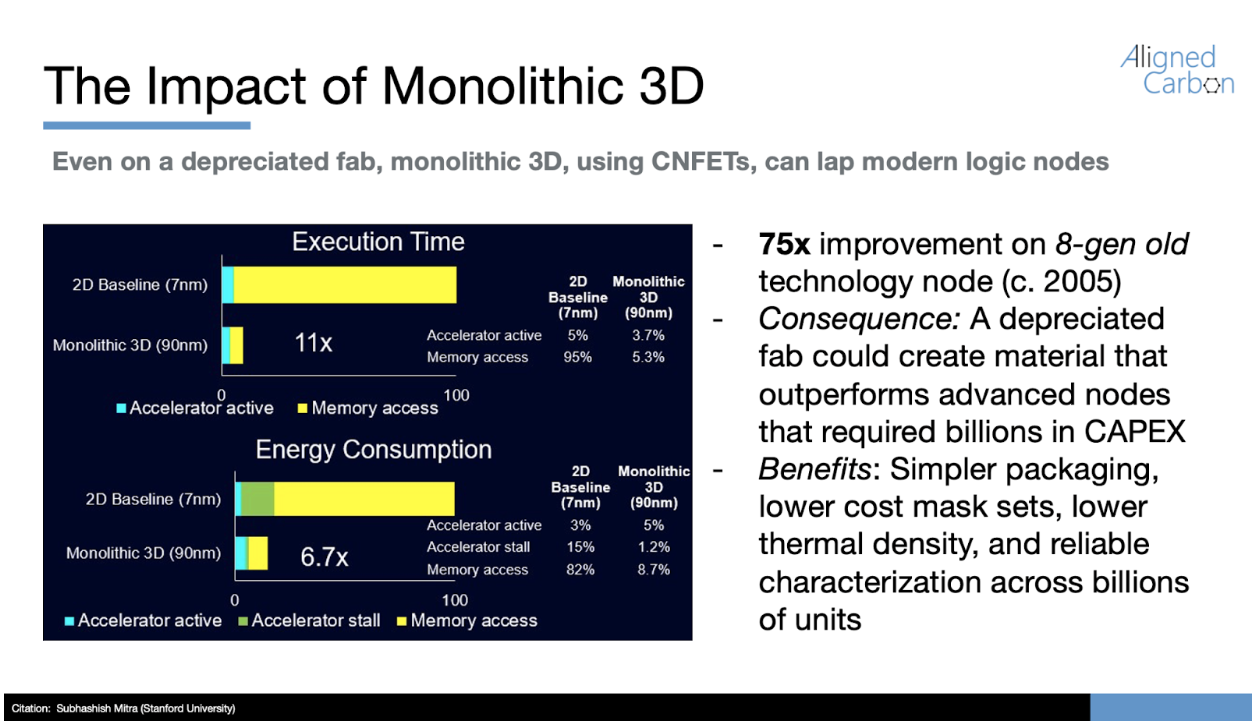
The importance of this cannot be overstated. In a high quality SPICE model analysis of what this would translate to at 5 nm technology, researchers at Stanford calculated, even including parasitic losses and other key “real world” losses, that a CNFET-on-SiFET monolithic 3D stack up could realize 1000x+ energy-delay compute gains, blasting well past Moore’s Law in the coming decades. Even using 90 nm node technology, CAPEX that foundries invested in all the way back in 2005, a CNFET-on-SiFET AI accelerator chip would observe a 75x energy-delay product compute improvement over TSMC’s 2021 state of the art 7 nm node technology. Consider that: Capital equipment from 2005 could be key in delivering a technology that beats the industry best today.
In the real world, what does this mean? If all logic in the world swapped to a technology with a 1000x energy-delay product improvement by 2030, this would translate to 4000 TWhr less electricity consumed, 1,500 GTonne less CO2 released, and $760B less spent on just electricity alone. Of course, this is a lovely picture to paint with very unrealistic expectations: Monolithic 3D will not even exit the foundry, based on best estimates, until 2030 or later, and adoption will not be immediate. Further, the 1000x gain assumes the best CNTs at the highest densities.
But the promise of this technology is nothing to balk at, and the semiconductor industry at large agrees. For instance, in its major roadmap release, IMEC announced how complementary FET technology, CFETs, will integrate into the expected stack up in the 2030s.
Now the question is: What technology is going to win? We believe in CNTs, and we hope you do too as we enter this journey. No matter what, one thing is for sure: Once we escape flatland, there is no going back to seeing the world as we did before.
About Aligned Carbon:
Aligned Carbon is a pioneering startup dedicated to revolutionizing the semiconductor industry by harnessing the power of carbon nanotube (CNTs). By providing the first ever semiconducting pure, aligned CNT wafers in a format compatible with the industry’s needs, Aligned Carbon serves as the key to unlocking next generation enhancements in monolithic 3D integration, energy efficient logic, sub-THz wireless, power electronics, and many other markets.
About Matti Thurston:
Matti Thurston is the Director of Product & Operations at Aligned Carbon. Mr. Thurston has expertise in translating materials level innovations into manufacturing scale products, with prior experience as an Engineering Program Manager in Apple’s Hardware Technology division as well as research experience in next-generation photonics, superconductors, and magnetic sensors. He received his MS in Materials Science from Stanford University and his BS from Cornell University.
Media Contact:
AC Comms Team
Follow Us on LinkedIn: https://www.linkedin.com/company/aligned-carbon/