Technology

Enabling the Semiconductor Industry to Enter Its New Material Age

Aligned Carbon's Alcar wafer platform enables the semiconductor industry to finally break free from the constraints of silicon, in so unlocking next generation planar FETs, monolithic 3D architectures, signal linearity in sub-THz frequency regimes, thermal and radiation stability enhancements, and many other material-level gains. Our material, provided in a foundry-compatible, wafer-scale format, is as plug-and-play as possible and ready for integration into your functional needs

Understanding the Power of CNTs

Carbon nanotubes have the ability to transform the semiconductor industry. This is true due to their remarkable physics, which can only be unlocked fully today on Aligned Carbon's ACNT wafer platform.

Unmatched Material Properties

Due to their atomic structure and carbon composition, CNTs demonstrate low resistivity for energy savings, high carrier mobility for enhanced clock speeds, high strength for stability, high thermal conductivity for efficient heat transfer, and radiation hardness, in comparison to Silicon.

Low Dimensional Structure

Given the atomic arrangement of CNTs, their form factor uniquely take a quasi one-dimensional form; this translates into no edge defects along the tube to scatter off of and, using our process, ordered arrangement, thereby providing a natural "gate all-around" material for future semiconductor chips

Foundry Friendly Processing

CNTs can be integrated into existing semiconductor processes, with benefits observed in both advanced node technologies and legacy node foundries; with a lower thermal processing window than Silicon, CNTs uniquely unlock monolithic 3D as well.

Our Unique Process

Aligned Carbon has developed its proprietary Alcar platform to provide the most valuable material possible for foundry integration. This means a three step process of aligned growth, purification, and transfer hinging on deep CNT expertise.

Aligned Wafer Scale Growth

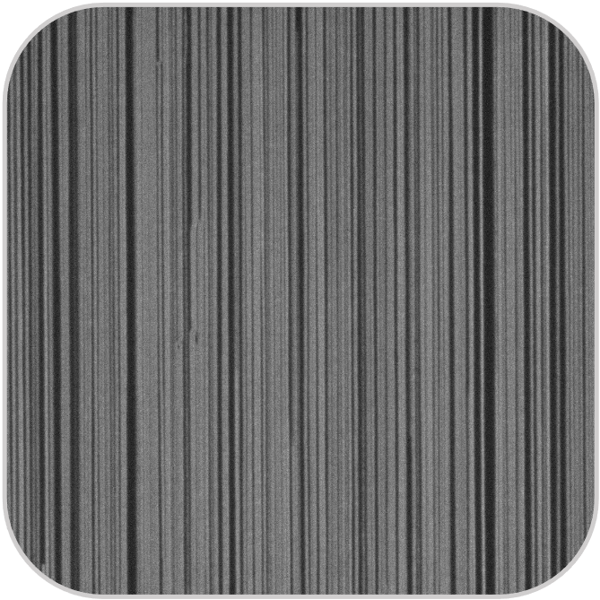
We utilize a unique wafer scale chemical vapor deposition (CVD) growth technique to achieve aligned CNTs. This ensures uniform density and effective scalability on all wafer sizes.

Semiconductor Purification

Our pathbreaking purification process utilizes a hybrid of technologies to ensure semiconducting purity while also maintaining alignment. We have achieved unprecedented purities that we are now sampling to strategic customers.

Target Wafer Auto Transfer

In order to enable monolithic 3D as well as multi-platform integration, CNT transfer is performed from our growth wafer to any target wafer. This means our process is scalable and deployable to essentially any substrate.
Monolithic 3D Integration

In order to realize truly revolutionary new efficiency improvements as well as brand new semiconductor use cases, material must evolve from planar designs into 3D designs. Monlithic 3D is uniquely unlocked by materials like carbon nanotubes.

Unlocked Applications

While monolithic 3D logic is one of the primary well-documented use cases for CNTs, the remarkable material properties available additional make CNTs valuable for analog / wireless technology, power electronics, sensors, quantum computers, and rad-hard microelectronics.

Let’s get aligned

We are working with innovation leaders, industry experts, and other key partners to enable this sea change in the semiconductor industry. Whether it is for demo wafer material, investment, partnership, or curiosity, we would love to talk.